The IIS Chip Gallery
Gemini (2012)

Additional pictures below, click to see larger versions

by


| Application | Cryptography |
| Technology | 180 |
| Manufacturer | UMC |
| Type | Master Thesis |
| Package | QFN56 |
| Dimensions | 1525μm x 1525μm |
| Gates | 100 kGE |
| Voltage | 1.8 V |
| Power | 263 mW, 125MHz 1.8V |
| Clock | 90 MHz |
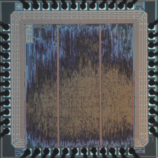
This ASIC implements the main multiplier for a 1233-bit eta-pi pairing.
This chip has one of the densest routing that we ever had in a design. To fit the design inthe given mini@sic area, we had to remove the lower I/O drivers. The bonding pads are still there, as we tried to keep the same bonding diagram as other designs, which saves us some money. But the pads do not connect to anything. Also note that, the design has only 100kGE and in theory has less area than Eva Longoria for example. If you compare the two designs you will notice that this is not the case. Another reminder that the GE is not really an accurate measure of the area.